Характеристики
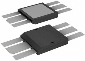
IXRFD630, Драйвер RF MOSFET, Low-Side, пиковый выходной ток 30АThe IXRFD630 is a CMOS high speed, high-current Gate Driver, specifically designed to drive MOSFETs in class D and E HF RF applications as well as other applications requiring ultrafast rise and fall times or short minimum pulse widths. The IXRFD630 can source and sink 30A of peak current while producing voltage rise and fall times of less than 4ns and minimum pulse widths of 8ns. The input of the driver is compatible with TTL or CMOS and is fully immune to latch up over the entire operating range. Designed with small internal delays, cross conduction or current shoot-through is virtually eliminated. The features and wide safety margin in operating voltage and power make the IXRFD630 unmatched in performance and value. The surface mount IXRFD630 is packaged in a low inductance RF package incorporating advanced layout techniques to minimize stray lead inductances for optimum switching performance.
• High Peak Output Current
• Low Output Impedance
• Low Quiescent Supply Current
• Low Propagation Delay
• High Capacitive Load Drive Capability
• Wide Operating Voltage Range
• High Power Surface Mount Design, Simplifying Mechanical Assembly of System
• Lowered Mechanical Stress ensures device floats on thermal compound, no induced package stress
• Economical high power mounting since mounting configuration don’t need machining of PCB or clamping
 Личный кабинет


 Загрузка