Характеристики
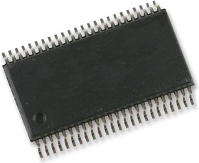
SN74ABT16245ADL, АП6The SN74ABT16245ADL is a 16-bit non-inverting 3-stage Bus Transceiver designed for synchronous 2-way communication between data buses. The control-function implementation minimizes external timing requirements. This device can be used as two 8-bit transceivers or one 16-bit transceiver. It allows data transmission from the A bus to the B bus or from the B bus to the A bus, depending on the logic level at the direction-control input. The output-enable input can be used to disable the device so that the buses are effectively isolated. When VCC is between 0 and 2.1V, the device is in the high-impedance state during power up or power down. However, to ensure the high-impendence state above 2.1V, OE should be tied to VCC through a pull-up resistor and the minimum value of the resistor is determined by the current-sinking capability of the driver. The SN74ABT16245A is characterized for operation from -40 to 85°C.
• State-of-the-Art EPIC-IIB™ BiCMOS design significantly reduces power dissipation
• Distributed VCC and GND pin configuration minimizes high-speed switching noise
• High-impedance state during power up and power down
• Flow-through architecture optimizes PCB layout
• High-drive outputs
• Latch-up performance exceeds 500mA per JESD 70
• Typical VOLP (output ground bounce)
 Личный кабинет


 Загрузка